Welcome to Shandong Wit Environmental Protection Technology Co.Ltd







Ultrapure Water Equipment for Semiconductor Manufacturing: Key Specifications Beyond Resistivity (TOC, Particle Count, Metals)
Sep 18, 2026
For semiconductor manufacturers, ultrapure water (UPW) equipment isn’t validated by resistivity alone. While >18.2 MΩ·cm is the textbook benchmark—and often the sole metric cited in procurement checklists—it reflects only ionic purity. In wafer fabrication, yield loss stems not from bulk conductivity, but from molecular-scale contaminants that evade resistivity measurement: organic carbon residues that nucleate micro-defects during photolithography; sub-20 nm particles that bridge gate structures or embed in dielectric layers; and metal ions like Fe, Ni, or Cu at ppt levels that catalyze oxidation or migrate under bias. These parameters—TOC, particle count, and metals—are not secondary specifications. They are primary failure vectors.
Total Organic Carbon (TOC) control demands more than just UV oxidation and degasification. TOC below 1 ppb requires suppression of leaching from piping materials (e.g., EPDM gaskets releasing extractables), elimination of biofilm niches in low-flow zones, and real-time monitoring with sub-ppb detection limits—not periodic grab sampling. Conventional UPW systems often fail here because they treat TOC as a post-polishing cleanup step rather than a system-wide design constraint. Material selection, flow dynamics, and surface passivation must be coordinated from pretreatment onward. A single elastomer seal or inadequately passivated stainless-steel weld can elevate TOC by 0.3–0.5 ppb during extended operation—enough to trigger defect spikes in 3nm node lithography.
Particle control presents a different challenge: it’s not about filtration alone, but about *particle generation*. Filters remove particles; UPW systems must prevent their formation. This hinges on mechanical stability—vibration-damped pumps, laminar-flow manifolds, and zero-turbulence valve actuation—and surface finish. Electropolished 316L SS with Ra < 0.4 µm reduces adhesion and shedding; non-metallic wetted parts (e.g., PFA-lined diaphragms) eliminate metallic wear debris. More critically, particle counters must be calibrated for sub-20 nm detection using NIST-traceable latex spheres—not just 50 nm or larger. Systems certified to SEMI F63 may report “<1 particle/mL @ ≥25 nm,” but that says nothing about the 10–19 nm range where EUV photoresist sensitivity peaks. True qualification requires in-line monitoring at multiple points: pre-UV, post-membrane, and at point-of-use—each with independent calibration and alarm thresholds tied to process excursion limits.
Metal contamination is the most insidious parameter. Resistivity masks ionic metals only when they’re fully dissociated and uniformly distributed. But in UPW distribution loops, localized corrosion—even microscopic pitting in weld heat-affected zones—releases transient metal bursts undetectable by bulk resistivity probes. These spikes deposit on wafers during rinse cycles, creating latent leakage paths. Effective control relies on three interdependent layers: first, material compatibility (e.g., titanium or high-purity PFA for critical loop sections); second, continuous online ICP-MS or electrochemical sensors capable of detecting Fe, Al, and Na at ≤10 ppt; third, dynamic passivation protocols—acidic or oxidative flushes timed to flow velocity and temperature—that stabilize oxide layers without introducing new contaminants. Static passivation alone is insufficient; it degrades under thermal cycling and flow interruption.
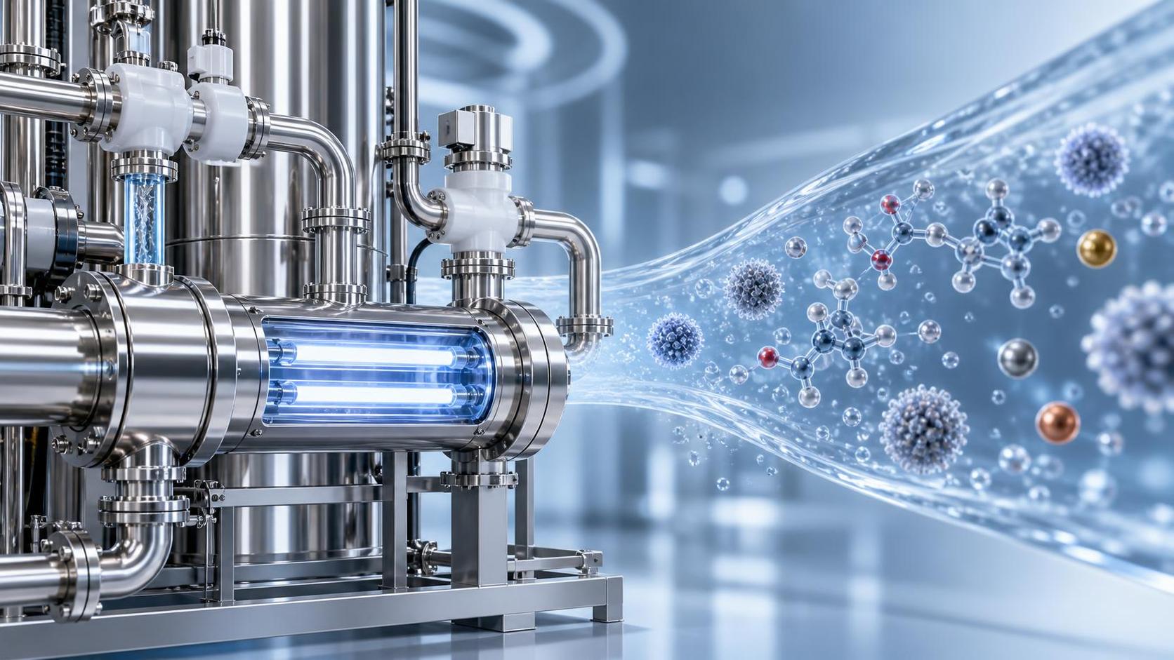
These requirements reshape system architecture. Pretreatment can no longer be treated as generic feedwater conditioning. Reverse osmosis membranes must reject not just divalent ions but also low-MW organics (e.g., dimethyl sulfoxide residuals from CMP slurry). Electrodeionization stacks require graded resin beds and current-density controls to avoid organic breakdown products. And final polishing stages must integrate dual-wavelength UV (185/254 nm) with catalytic oxidation—not just photolysis—to mineralize persistent compounds like perfluorinated surfactants.
This level of integration explains why UPW systems for advanced fabs increasingly diverge from standard pharmaceutical or power-generation designs. It also clarifies why environmental technology firms with deep process-water expertise—particularly those with proven experience in high-integrity, low-leachability systems for regulated industries—bring transferable rigor to UPW engineering. For instance, technologies developed for chlorine dioxide generation under stringent purity constraints—such as the W1 type (low negative pressure) chlorine dioxide preparation technology—demonstrate how precise chemical dosing, inert material selection, and real-time residual monitoring translate across critical water applications. The same principles of trace-metal avoidance, organic minimization, and particle suppression apply whether disinfecting ultrapure rinse water or generating oxidant for clean-in-place cycles.
Ultimately, UPW equipment validation must shift from compliance-driven testing to physics-based failure modeling. If a particle counter reads “0” but wafer defect maps show periodic clustering, the issue lies not in the sensor—but in unmodeled flow-induced shedding. If TOC stays flat while yield drops, the culprit may be non-oxidizable organosilicon compounds slipping past UV reactors. Resistivity remains necessary—but it is no longer sufficient. The real specification is not a number. It’s the absence of measurable impact on device performance across thousands of wafers. That demands instrumentation, materials science, and system-level thinking—not just another checkbox on a spec sheet.


Previous:No more content
Next:No more content
News Recommended
 How Ultrapure Water Equipment Validates Compliance with SEMI F63-1118 for 28nm+ Wafer Fabrication
") Ultrapure Water Equipment for Semiconductor Manufacturing: Key Specifications Beyond Resistivity (TOC, Particle Count, Metals)
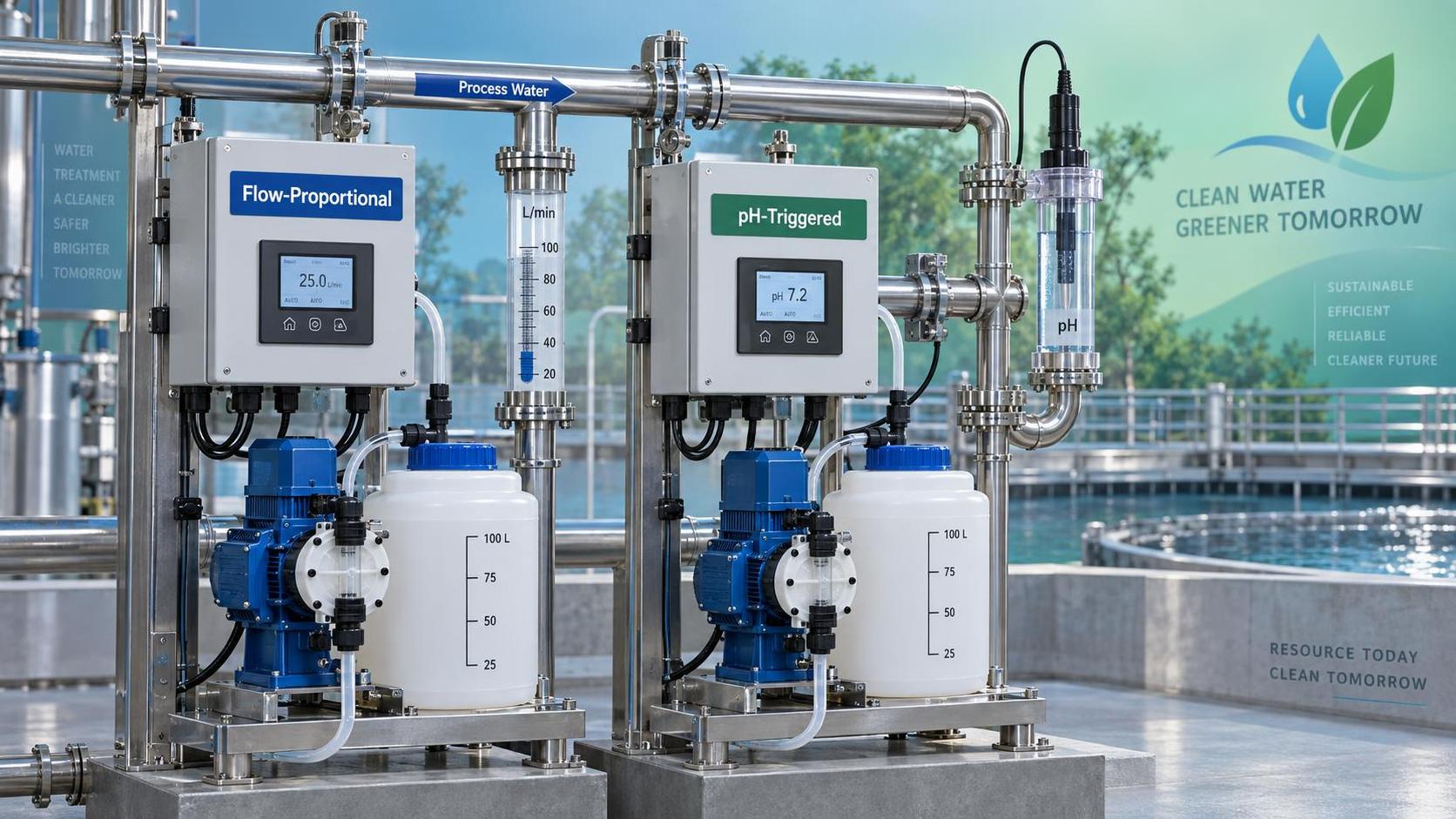
Ultrapure Water Equipment for Semiconductor Manufacturing: Key Specifications Beyond Resistivity (TOC, Particle Count, Metals) Why Flow-Proportional vs. pH-Triggered Automatic Dosing Units Deliver Different Outcomes in Wastewater Neutralization
 Automatic Dosing Unit Selection Guide: Matching Pump Type, Control Logic, and Calibration Accuracy to Your Water Matrix
 How Sodium Chlorite Generators Work: Electrochemical Generation, Feedstock Purity Requirements, and Output Stability Control
 Sodium Chlorite Generator vs. Bulk Chemical Delivery: Total Cost of Ownership for On-Site Disinfectant Production
GET A FREE QUOTE
Service Commitment: Upon receipt of your message, a dedicated representative will contact you as soon as possible to provide efficient and professional service support.
